Contributing to a new world with 3D semiconductor integration technology

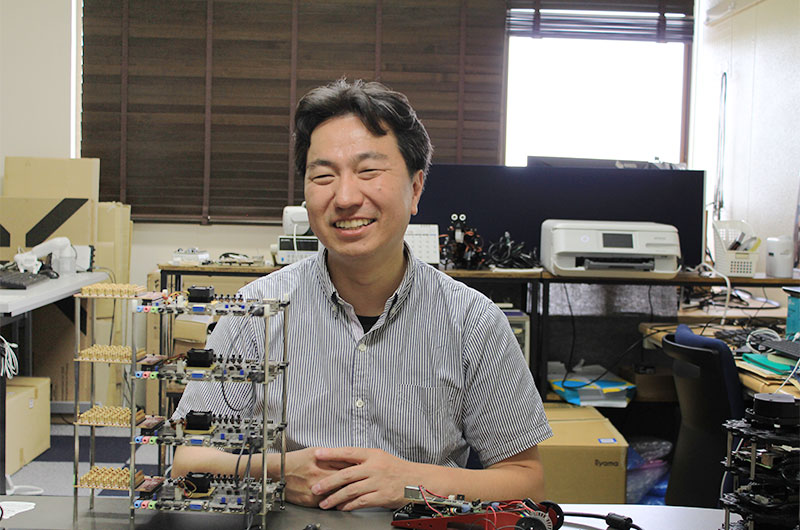
Dr. Takeshi OHKAWA, Associate Professor
Research and Education Institute for Semiconductors and Informatics
Kumamoto is now attracting semiconductor-related companies, which will revitalize the local economy. To support this movement, Kumamoto University is actively collaborating with universities and industries in Japan and overseas and is focusing its efforts on research into new semiconductor processes, such as by establishing the Research and Education Institute for Semiconductors and Informatics (REISI). In this article, Associate Professor Takeshi Okawa, who is researching the world-renowned 3D stacking technology for semiconductors , talks about his work.
Researching 3D integration technology to create more functions on a semiconductor chip
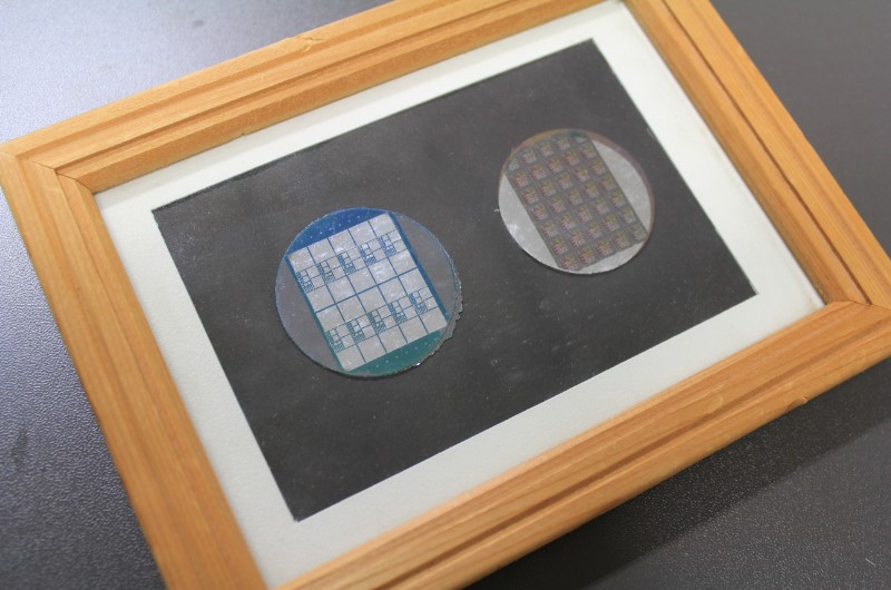
What kind of research are you doing?Dr. Ohkawa: Simply put, it is the study of semiconductor chips. Semiconductor chips are made by creating circuits on the surface of a plate called a silicon wafer and building in various functions. Until now, very thin wiring and small components have been used to provide many functions. However, as devices continue to get smaller, conventional methods are reaching their limits.
In response, attention is turning to 3D integration technology, in which chips are stacked on top of each other to create a system. Not only does this technology make systems more compact, but it is also expected to make it possible to build in more functions than ever before when the system is well structured. Kumamoto University is in the process of trying to take advantage of this technology to create a system that has strengths in packaging technology that allows multiple semiconductors to interact with each other and work as if they were a single semiconductor.
There are two major types of semiconductor research: the hardware part and the software part. I am mainly working on the software part, which is how to design the system. I am researching what kind of system can be created when the chips are connected.
What will be possible when the system is put to practical use?
Dr. Ohkawa: Our current target is robots, and by using a 3D integration system, we can build more compact systems than ever before. We can expect applications such as AI to recognize images and link them to robot movements. For example, a system that simply captures an image with a camera, recognizes what kind of object it is, and performs processing such as moving the necessary motors would be possible.
I also expect this technology to be applied in the IoT (Internet of Things) field. For example, in the field of agriculture, a system could use sensors to acquire data on temperature, moisture, wind, etc. at various locations, and send the processed data via the Internet. With current technology, the size of system is about the size of a lunch box, but with a 3D integration system, it can be made as small as a grain of rice. Since the system can be installed in many locations, it is expected to improve the accuracy of information and reduce costs.
My first excitement was the joy of seeing what I had programmed appear on the screen.
When did you first become interested in fields such as semiconductors?Dr. Ohkawa: I started my research on semiconductors when I joined a semiconductor research laboratory at university, where I studied design automation of field programmable gate array (FPGA) integrated circuits. It was basic research on how to effectively link hardware (i.e. integrated circuits) and software to achieve high performance with low power consumption. I started research on 3D stacking in earnest when I moved to Kumamoto University.
Have you always been interested in programming and computers?
Dr. Ohkawa: I first became interested in programming and computers when I was in the early grades of elementary school. My father bought me an 8-bit computer at the time. It was right around the time when home computer games were just starting to be released. I was not allowed to buy a game console, so I enjoyed writing programs on the computer and making this like games. It was simple ones, just a few characters appearing and you could move them with the keyboard, but I was fascinated by fact that the computer worked as I had programmed it to. Later, I will never forget the excitement when dots appeared on the screen using a programming language (assembler) that the microprocessor itself interpreted. This was my first excitement, and it has led me to where I am today.
Creating useful products for the world, while being stimulated by the serious eyes of companies.
Your laboratory is also involved in joint research with companies, isn’t it?
Dr. Ohkawa: We are working with a local company to standardize 3D integration technology. We would like to expand our ideas to the world. The companies we are working with are very active and very interesting.
I learn a lot from the feedback from the companies from their serious viewpoints. I feel it is a win-win situation.
Any comments for the students?
Dr. Ohkawa: When thinking about a research theme, I think it is not interesting to come up with something that already exists in the world today. It is interesting to think about what kind of things would be useful to the world and what kind of things would be useful to developers in the world. Perhaps that is what research is all about.
For this reason, I want you to be aware of your output. For example, ask your friends to look at what you have created. By having them look at it from a different perspective, not only will you get new ideas, but you will also be able to see your own growth and what you are good at. It may be difficult to see what you want to do as a high school or undergraduate student, but if you try to make it visible, I am sure you will be able to understand.
We can also introduce books and other materials to students who do not belong to our research lab, saying “Here are some interesting ones.” Please do not hesitate to ask.
Related links: